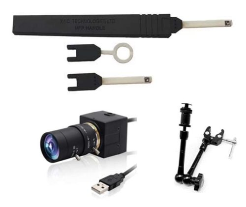
YIC NFP E and H Field Probe KIT
Key Features and Functions
- Fully integrated with Y.I.C. Technologies EMViewer and EMProbe
- Live real-time probe position tracking
- Normalization and correction when using the EMViewer software
- Flat response within the range of operation
- Slim Design and Protective Coating
- 18GHz Measured Cable included
Applications:
EMC/EMI Pre-Compliance Magnetic Near-Field Measurements
- Magnetic Near Field mapping
- Magnetic Immunity Testing
Y.I.C. Technologies set of EM probes kit designed for measuring near field radiated emissions for EMC/EMI pre-compliance testing.
The probes can be used to locate, identify, measure and characterize potential sources of electromagnetic radiation and interference radiated from traces or components of electronic PCBs, assemblies or products. The probe output is proportional to the magnetic field (H) strength present at the probe location.
A compatible Spectrum Analyzer with 50Ω input is required and the probes can be used as handheld standalone probes or mounted on Y.I.C. Technologies EMProbe robotic arm for high resolution scans.
Ideal PCB projects for EMScanner are boards designed for high speed, high power, and/or high density/complexity. Any PCB that places a premium on board real-estate also qualifies as an excellent candidate. The compact, flat scanner provides PCB design teams with an easy-to-use, costeffective, and proven tabletop solution. Emission, immunity, filtering, EMI shielding, broadband noise and Common Mode testing are some of the applications that the EMScanner system addresses in mere seconds.
Live tracking provides a faster, easier, and more reliable method to get these results. Using an overhead webcam and probe markers, EMViewer will detect the type of probe and point of measurement automatically, allowing design engineers to see results quickly with minimal setup time.


