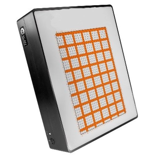
EMScanner R High speed 8GHz High Resolution EMC and EMI diagnostic tool
Scanner Specifications:
- Broadband frequency coverage: To 8 GHz
- Antenna array: 1,218 (42 x 29) H-field probes
- Build-in spectrum analyzer
- Spatial resolution: 8 levels of resolution (60 microns – 7.5 mm)
- Scan area: L 31.6 cm x W 21.8 cm (L 12.44” x W 8.58”)
- Frequency accuracy of peaks: Peak marking accuracy of spectrum analyzer
- Probe to probe uniformity: Calibrated before shipment. Firmware correction factors adjust for frequency dependent probe responses with +/- 3 dB accuracy
- Measurement plane isolation: > 20 dB
- Maximum radiated power load: 10 W / 40 dBm
- Enclosure Anodized non-conductive metal
- Maximum DUT voltage Glass Cover: 4kV DC; 2.6kV AC | Metal Case: 260V DC; 200V AC (measured as dielectric withstanding voltage - DWV)
- Operating temperature: From -20 °C to +45 °C (continuous spectral and spatial scans at 50 MHz)
High resolution EMC and EMI testing has never been this fast!
World’s fastest EMC/EMI diagnostic system has been reinvented to assist high density board designers to visualize the root causes of potential EMC and EMI problems during pre- and post EMC compliance testing.
EMScannerR+ enables the PCB and design engineers to diagnose EMC/EMI problems between 150 kHz and 8 GHz. EMScanner+ provides 8 levels of resolution (60 microns – 7.5 mm). Level 1 resolution (7.5 mm) allows the engineers to visualize the hot spots, current loops or intermittent problems in real-time. After locating the unintended radiators, engineers can zoom into the problem by selecting the resolution level based on the density of the board design.
There is no need for an external spectrum analyzer to run EMScannerR+. Built-in spectrum analyzer turns EMScannerR+ into a plug-and-play test system.
EMScannerR+ provides unique pre- and post-EMC compliance testing that images emissions. During any new PCB development process, design engineers must find, characterize, and address unintended radiators or RF leakage to pass compliance testing. EMScannerR+ allows board designers to pre-test and resolve EMC and EMI problems early on, thus avoiding unexpected EMC compliance test results.
EMScannerR+ quickly delivers repeatable and reliable results that pinpoint the cause of a design failure. As a result, the user can personally test the design without having to rely on another department, test engineer, or time-consuming off-site testing. After diagnosing even an intermittent problem, the engineer can implement a design change and retest. The results provide concrete verification of the effectiveness (or not) of the design change.


