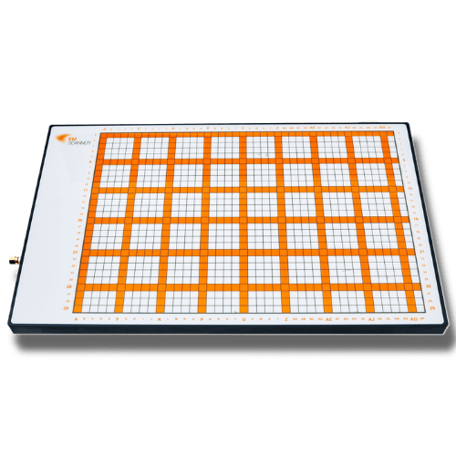
EMScanner High speed 8GHz Real-time EMC and EMI diagnostic tool
Scanner Specifications:
- Broadband frequency coverage: To 8 GHz
- Antenna array: 1,218 (42 x 29) H-field probes
- Build-in spectrum analyzer
- Spatial resolution: 8 levels of resolution (60 microns – 7.5 mm)
- Scan area: L 31.6 cm x W 21.8 cm (L 12.44” x W 8.58”)
- Frequency accuracy of peaks: Peak marking accuracy of spectrum analyzer
- Probe to probe uniformity: Calibrated before shipment. Firmware correction factors adjust for frequency dependent probe responses with +/- 3 dB accuracy
- Measurement plane isolation: > 20 dB
- Maximum radiated power load: 10 W / 40 dBm
- Enclosure Anodized non-conductive metal
- Maximum DUT voltage Glass Cover: 4kV DC; 2.6kV AC | Metal Case: 260V DC; 200V AC (measured as dielectric withstanding voltage - DWV)
- Operating temperature: From -20 ?C to +45 ?C (continuous spectral and spatial scans at 50 MHz)
EMC and signal integrity are major concerns in the design of ultra-high speed (>2 GHz) PCBs. EMScanner enables the design engineers to diagnose EMC/EMI problems between 150 kHz and 8 GHz.
The EMScanner provides unique pre- and post- EMC compliance testing that images real-time emissions. EMScanner allows engineers to visualize the root causes of potential EMC and EMI problems.
During any new PCB development process, design engineers must find, characterize, and address unintended radiators or RF leakage to pass compliance testing. EMScanner allows board designers to pre-test and resolve EMC and EMI problems early on, thus avoiding unexpected EMC compliance test results.
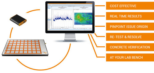
EMScanner delivers repeatable and reliable results that pinpoint in less than a second the cause of a design failure. As a result, the user can personally test the design without having to rely on another department, test engineer, or time-consuming off-site testing. After diagnosing even an intermittent problem, the engineer can implement a design change and retest. The results provide concrete verification of the effectiveness (or not) of the design change.
EMScanner consists of a patented scanner and compact adaptor, and of a customersupplied spectrum analyser and PC running EMScanner software. EMScanner diagnostic capabilities allow design teams to reduce testing time by more than two orders of magnitude. Users have also documented fifty percent reductions in design cycle times.


